Chips on most modern desktops have four cores, but chip manufacturers have already announced plans to migrate to six cores, and for high-end servers, even today 16-core processors are far from uncommon.
The more cores there are, the greater the problem of memory allocation between all cores while working together. With the increase in the number of cores, it is increasingly beneficial to minimize the loss of time on managing the cores during data processing - because the data exchange rate lags behind the processor speed and data processing in memory. You can physically turn to someone else's fast cache, or you can go to your slow cache, but save time on data transfer. The task is complicated by the fact that the memory requested by the programs does not clearly correspond to the cache sizes of each type.
Only a very limited amount of memory can physically be placed as close as possible to the processor — the L1 processor cache, which is extremely small. Daniel Sanchez, Po-An Tsai, and Nathan Beckmann — researchers at the laboratory of computer science and artificial intelligence at the Massachusetts Institute of Technology —
taught the computer to configure different kinds of memory under a flexible hierarchy of programs in real time mode. The new system, called Jenga, analyzes the volume requirements and the frequency of programs accessing memory and redistributes the power of each of the 3 types of processor cache in combinations that provide increased efficiency and energy savings.

To begin with, the researchers tested the performance increase with a combination of static and dynamic memory in the work on programs for a single-core processor and obtained a primary hierarchy - which combination is better to use. From 2 types of memory or from one. Two parameters were estimated: signal delay (latency) and energy consumption during the operation of each program. Approximately 40% of programs began to work worse with a combination of memory types, the rest - better. Having fixed which programs “love” mixed performance and which memory size, the researchers built their Jenga system.
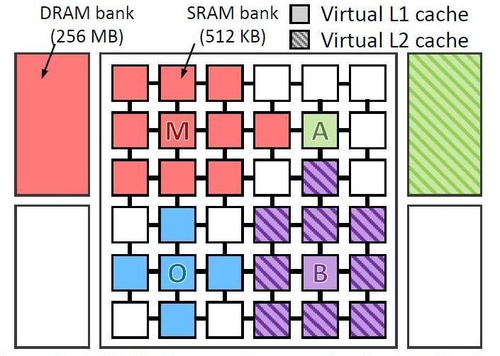
They virtually tested 4 types of programs on a virtual computer with 36 cores. Tested programs:
- omnet - Objective Modular Network Testbed, Modeling Library C and Network Modeling Platform (blue color in the figure)
- mcf - Meta Content Framework (red)
- astar - software for displaying virtual reality (green)
- bzip2 - archiver (purple)

The picture shows where and how the data of each program was processed. The letters show where each application runs (one per quadrant), the colors show where its data is located, and the hatching indicates the second level of the virtual hierarchy when it is present.
Cache levelsCPU cache is divided into several levels. For universal processors - up to 3. The fastest memory is the first level cache - L1-cache, because it is located on the same chip as the processor. Consists of instruction cache and data cache. Some processors without L1 cache cannot function. L1 cache runs at the processor frequency, and can be accessed every clock cycle. It is often possible to perform several read / write operations at the same time. The volume is usually small - no more than 128 KB.
The second level cache interacts with the L1 cache - L2. He is the second in speed. It is usually located either on a chip, like L1, or in close proximity to the core, for example, in a processor cartridge. In older processors, the chipset on the motherboard. L2 cache size from 128 KB to 12 MB. In modern multi-core processors, the second-level cache, being on the same chip, is a separate-use memory — with a total cache size of 8 MB per core accounts for 2 MB. Usually, the L2 cache latency located on the core chip is from 8 to 20 core cycles. In the tasks associated with numerous calls to a limited memory area, for example, a DBMS, its full-fledged use gives rise to productivity tenfold.
The L3 cache is usually even bigger in size, although somewhat slower than the L2 (due to the fact that the bus between L2 and L3 is narrower than the bus between L1 and L2). L3 is usually located separately from the CPU core, but can be large — more than 32 MB. L3 cache is slower than previous caches, but still faster than RAM. In multiprocessor systems is in common use. The use of a third-level cache is justified in a very narrow circle of tasks and may not only not give an increase in performance, but vice versa and lead to an overall decrease in system performance.
Disabling the cache of the second and third levels is most useful in mathematical problems when the amount of data is less than the size of the cache. In this case, you can load all the data at once into the L1 cache, and then process it.
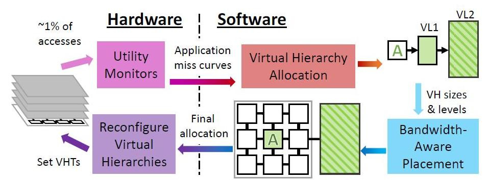
Periodically, Jenga at the OS level reconfigures virtual hierarchies to minimize the volume of data exchange, given the limited resources and application behavior. Each reconfiguration consists of four steps.

Jenga distributes data not only depending on which programs are dispatched — those who love large single-speed memory or those who love the speed of mixed caches, but also depending on the physical proximity of the memory cells to the data being processed. Regardless of what kind of cache the program requires by default or hierarchy. The main thing is to minimize signal delay and energy costs. Depending on how many types of memory the program loves, Jenga models the latency of each virtual hierarchy with one or two levels. Two-level hierarchies form a surface, single-level hierarchies - a curve. Jenga then designs the minimum delay in VL1 sizes, which gives two curves. Finally, Jenga uses these curves to select the best hierarchy (i.e., the size of VL1).
The use of Jenga gave a tangible effect. The virtual 36-core chip began to work 30 percent faster and used 85 percent less energy. Of course, while Jenga is just a simulation of a working computer and it will take some time before you see real examples of this cache and even before chip makers accept it if you like the technology.
Configuration of conditional 36 nuclear machine
- Processors 36 cores, x86-64 ISA, 2.4 GHz, Silvermont-like OOO: 8B-wide
ifetch; 2-level bpred with 512 × 10-bit BHSRs + 1024 × 2-bit PHT, 2-way decode / issue / rename / commit, 32-entry IQ and ROB, 10-entry LQ, 16-entry SQ; 371 pJ / instruction, 163 mW / core static power - L1 caches . 32 KB, 8-way set-associative, split data and instruction caches,
3-cycle latency; 15/33 pJ per hit / miss - Prefetchers Prefetch Service 16-entry stream prefetchers modeled after and validated against
Nehalem - L2 caches . 128 KB private per-core, 8-way set-associative, inclusive, 6-cycle latency; 46/93 pJ per hit / miss
- Coherent mode (Coherence) . 16-way, 6-cycle latency directory banks for Jenga; in-cache L3 directories for others
- Global NoC . 6 × 6 mesh, 128-bit flits and links, XY routing, 2-cycle pipelined routers, 1-cycle links; 63/71 pJ per router / link flit traversal, 12 / 4mW router / link static power
- Static SRAM blocks . 18 MB, one 512 KB bank per tile, 4-way 52-candidate zcache, 9-cycle bank latency, Vantage partitioning; 240/500 pJ per hit / miss, 28 mW / bank static power
- Stacked DRAM multi-layer dynamic memory . 1152MB, 128MB one vault per 4 tiles, Alloy with MAP-I DDR3-3200 (1600MHz), 128-bit bus, 16 ranks, 8 banks / rank, 2 KB row buffer; 4.4 / 6.2 nJ per hit / miss, 88 mW / vault static power
- Main memory . 4 DDR3-1600 channels, 64-bit bus, 2 ranks / channel, 8 banks / rank, 8 KB row buffer; 20 nJ / access, 4W static power
- DRAM timings . tCAS = 8, tRCD = 8, tRTP = 4, tRAS = 24, tRP = 8, tRRD = 4, tWTR = 4, tWR = 8, tFAW = 18 (all timings in tCK; stacked DRAM has the tcK as main memory )